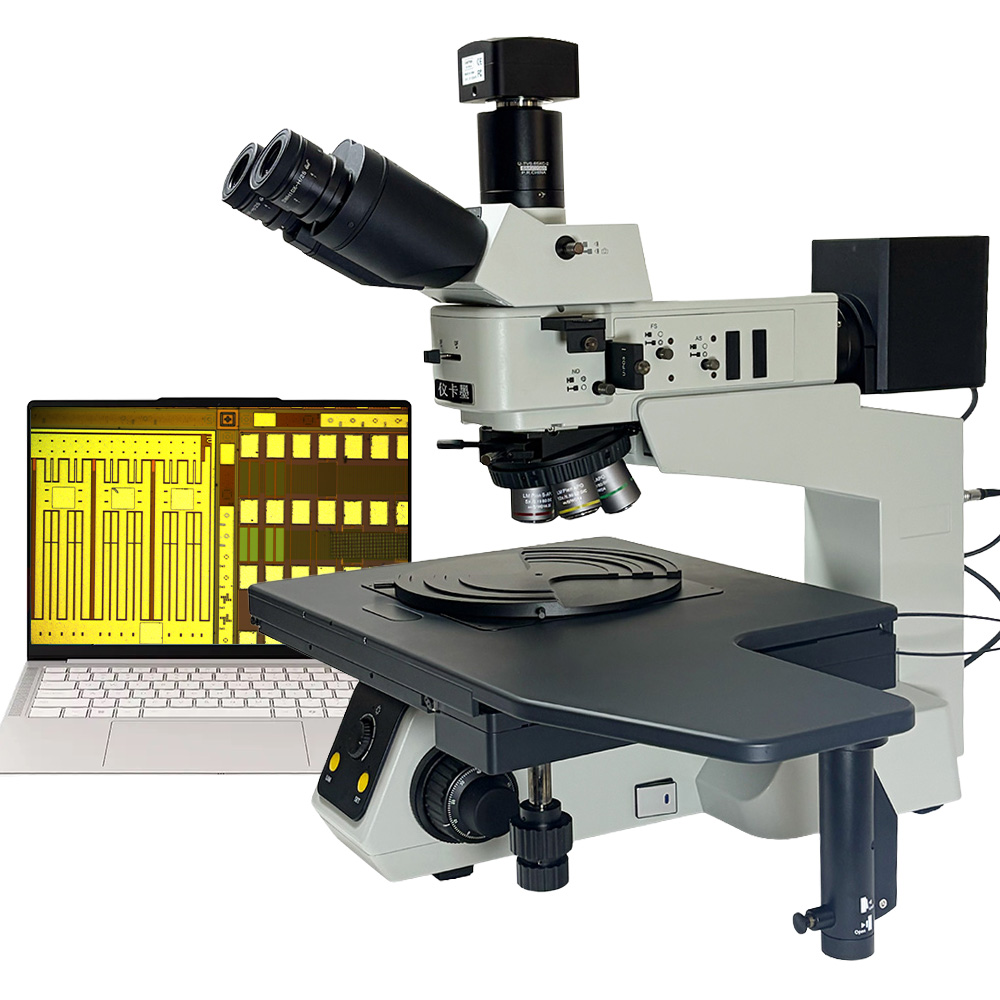
Wafer inspection requires a microscope that can hold a full wafer, move across it without re-clamping, and resolve defects that are small in both lateral size and contrast: particles, scratches, residues, edge chipping and thin-film non-uniformity.
Yikmo builds wafer inspection microscopes with 8-inch stages, 210 × 210 mm travel, long working distance darkfield objectives and optional DIC.
A polished wafer is mirror-like. In brightfield, a particle or a scratch scatters light away from the objective and can disappear against the bright background. In darkfield, the specular reflection is blocked and only scattered light is collected, so particles, scratches and edge defects appear bright against a dark background.
DIC adds topography contrast by comparing the optical path difference between two closely spaced points. It is used for step heights, shallow pits and surface roughness rather than for particles.
| Stage travel | For 8-inch (200 mm) wafers you need at least 210 × 210 mm travel; a 12-inch wafer needs a larger stage or a wafer loader. |
|---|---|
| Working distance | Long working distance objectives (8–15 mm) leave room for probes and fixtures and reduce the risk of contact. |
| Contrast | Darkfield is essential for particles and scratches; DIC for topography; polarized light for films and stress. |
| Cleanliness | The stage and objectives should be easy to clean, and the stand should minimise particle generation. |
At least 210 × 210 mm of travel, plus a stage plate large enough to support the wafer without overhang.
You can inspect small pieces, but a standard 75 × 50 mm stage cannot cover a full wafer without re-clamping, which risks damage and slows inspection.
Typically 50×–500×. Low magnification for scanning and locating defects, higher magnification for classification and measurement.
Send us the material and what you need to measure. We reply within one business day with a specification and quotation.